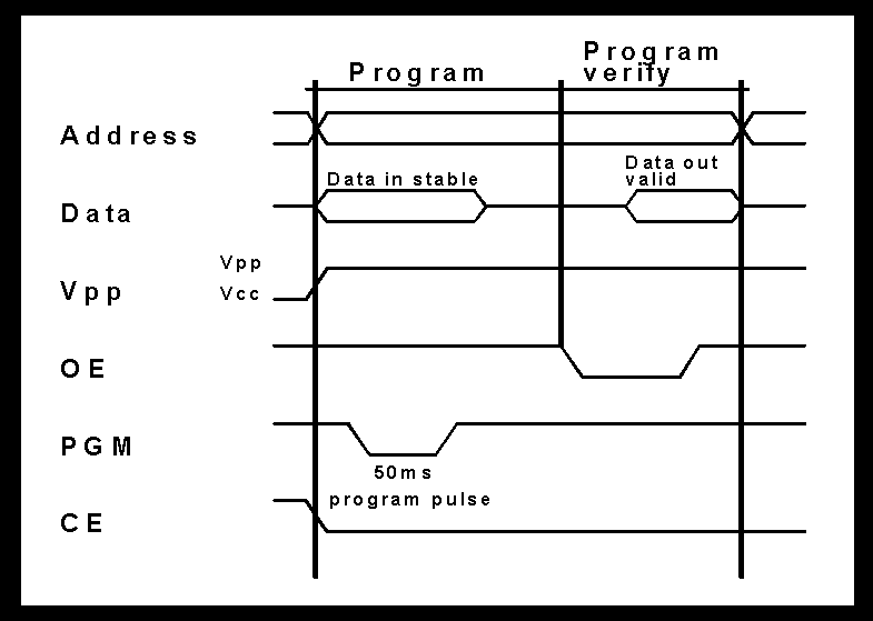
EPROM ( Erasable Programmable Read Only Memory) is logic device which can be used as ordinary memory structure or as complex logic structure (used to realize a various logic function's). Once programmed content of EPROM can not be altered: it can be only used as ROM (read only) memory in normal working conditions. However, it's possible to reprogram EPROM by erasing the whole content of it and then entering in so called program mode which allows programming of EPROM (writing desired data in EPROM). Erasure of EPROM is performed by UV-light: the transparent lid allows the user to expose the chip to ultraviolent light to erase bit pattern. Programming of EPROM is performed by applying high voltage (~21v), bringing desired address and data bits on specified pins and by changing control signals (OE,CE,PGM) in determined program pulse. There are two ways of programming EPROM:
Simple programming is programming which is used to program EPROM of lower capacity (8192 x 8bit-27128 or 4096 x 8bit-2764). It uses a wide program pulse (~50ms) which results that programming takes longer time (including verifying).
High performance programming is used to program EPROM's of larger capacity (27256, 27512,..). It is quick and reliably programming performed by so called "intelligent" high performance programators. Note: you can't program every EPROM chip by this method because the chip must support this kind of programming.
High performance programators are much more expensive then simple programatars but they provides users with variety of functions: -they can program other PLD devices such are GAL, EEPROM, PIC 16xx microchips. -they can be adjusted to program any new PLD device (they have ability to adapt voltage levels to new chips and to change functions of pins). It means that user have to purchase new software (which comes with new type of PLD) to program that new PLD so he doesn't have to purchase whole new programator. Example: GALEP for PC is high performance programator which can program 8-bit EPROMs (max 32 pin), 16-bit EPROMs (max 40 pin), Flash EPROMs, EEPROMs, serial EEPROMs, GALs, microcontrollers 87 x 51/52 and microchip PIC 16xx. Programming 27C512 (64Kb) EPROM takes about 13sec. Price: 698DEM (Deutch Marks) Source:CONRAD Electronic Hauptkatalog 97.
Marks for EPROM chips 27128: first two numbers tells us that it's UV-erasable EPROM, other three numbers are capacity of EPROM in Kbits:128Kbits=16384 x 8bit (16Kbyte). Note: EPROM can be also organized as 16bit matrix or 4bit matrix. 27C512: "C" means that EPROM is manufactured in CMOS technology. Example: HN27C64G-15: 8Kb (8192x8bit) UV-erasable EPROM in CMOS technology made by HITACHI (mark "HN") with 150ns access time (mark "-15").
Price 27128 (16K x 8) with access time of 200ns:11.5DEM 27512 (64K x 8) with access time of 200ns:16.95DEM 27C512 (64K x 8) with access time of 150ns:8.95DEM 27C1024 (64K x 16) with access time of 150ns:16.95DEM Source:CONRAD Electronic Hauptkatalog 97.
Pin outs
A0-A1
Addresses
CE
Chip enable
OE
Output enable
D0-D7
Data
PGM
Program
Vcc,Vpp
Power
Note: On picture is 27128 16Kb EPROM . 2764 EPROM has same configuration of pins, but it doesn't has "A13" (that pin is marked as "N.C.":not connected). 27256 EPROM also has same pin configuration but instead of PGM it has pin marked "A14" (it doesn't has PGM).
Comparison between HN27128G-25and HN27C256G-20
HN27128G-25
HN27128G-25 is 16Kbyte UV erasable EPROM which supports both simple and high performance programming. Features:
Single power supply: +5v +/-5%
Simple programming: -Program voltage: Vpp=+21v DC -Program with One 50ms pulse
Static: -No clock required -Inputs and outputs TTL compatible during both read and program mode
Access time: 250ns
Low stand-by current: 35mA
Absolute max. rating of Vpp pin 26.5v
High performance programming available
Compatible with INTEL 27128
Mode selection
Mode\Pin
CE (20)
OE (22)
PGM(27)
Vpp (1)
Vcc (28)
Outputs
Read
VL
VL
VH
Vcc
Vcc
Dout
Stand by
VH
x
x
Vcc
Vcc
High Z
Program
VL
x
VL
Vpp
Vcc
Din
Pr. verify
VL
VL
VH
Vpp
Vcc
Dout
Pr. inhibit
VH
x
x
Vpp
Vcc
High Z
Note: VL - low voltage (logic "0") level VH - high voltage (logic "1") level x - don't care Vpp - program voltage +21v Vcc - +5v High Z - high impedance
Simple programming time diagram
HN27256G-20
HN27256G-20 is 32Kbyte EPROM manufactured in CMOS technology providing very low power dissipation. Features:
Low power dissipation: -20mW/Mhz (Active mode) -5microW (Standby mode)
Access time: 200ns
Single power supply: +5v +/-5%
High performance programming: -program voltage: +12.5v DC
Static: -No clock required -Inputs and outputs TTL compatible during both read and program mode
Absolute max. rating of Vpp pin 14.0v
Compatible with INTEL 27256
Mode selection
Mode\pin
CE (20)
OE (22)
Vpp (1)
Vcc(28)
Outputs
Read
VL
VL
Vcc
Vcc
Dout
Out. disable
VL
VH
Vcc
Vcc
High Z
Standby
VH
x
Vcc
Vcc
High Z
Program
VL
VH
Vpp
Vcc
Din
Pr. verify
VH
VL
Vpp
Vcc
Dout
Opt. verify
VL
VL
Vpp
Vcc
Dout
Pr. inhibit
VH
VH
Vpp
Vcc
High Z
Note: VL - low voltage (logic "0") level VH - high voltage (logic "1") level x - don't care Vpp - program voltage +12.5v Vcc - +5v High Z - high impedance
High performance programming time diagram
Note: You can see that this diagram isn't much different then simple prog. diagram but main difference is that all signals at high performance prog. are much shorter. (quicker programming).
EEPROM
Electrically erasable and programmable ROM (EEPROM) are programmable logic devices having similar characteristics as ordinary EPROM. Main difference and main advantage of EEPROM is that they can be electrically erased with possibility to erase specified byte within contest of chip ( not whole contest of chip like ordinary EPROM). Because of that they are widely use in various modern electronic devices. E.G. Within TV-sets they are used for memorizing current volume, program channels and other parameters. Even if the TV is unplugged from power source these parameters are preserved in EEPROM. When user changes these parameters he actually reprograms EEPROM in TV (or PC-monitor). Disadvantages of these devices are that they are expensive and they have high power dissipation.
Price 28C64 (8K x 8) 250ns: 17.95DEM 28C256 (32K x 8) 150ns: 49.90DEM
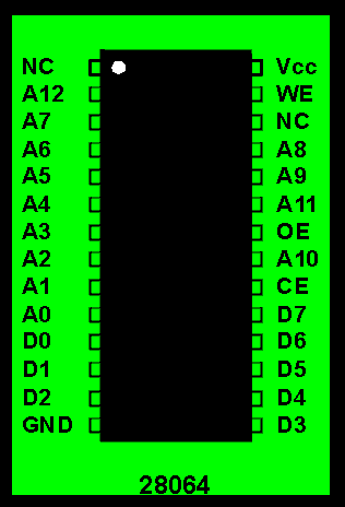
Example: HN28064P-25 (HITACHI)
Pin outs
A0-A1
Addresses
CE
Chip enable
OE
Output enable
D0-D7
Data
WE
Write enable
Vcc
Power
Features:
Single 5v supply
Address, data CE, OE latches
Byte erase / write time: 10ms typ.
Chip erase time: 20ms typ.
Fast access time: 250ns
Low power dissipation: -300mW (Active) -125mW (Standby)
Conforms to JEDEC Byte-Wide Standard
Reliable N-channel MNOS technology
1000 erase/write cycles
Mode selection
Mode\pin
CE (20)
OE (22)
WE (27)
Data
Read
VL
VL
VH
Dout
Standby
VH
x
x
High Z
Byte erase
VL
VH
VL
Din=VH
Byte write
VL
VH
VL
Din
Chip erase
VL
VL
VL
Din=VH
Deselect
VL
VH
VH
High Z
GAL
Generic Array Logic (GAL) is programmable logic device ( CMOS technology) using EEPROM controlling bits providing electrically erasing and programming. The main function of GAL is to substitute two, three or more ordinary logic circuits (AND, NAND, NOT gates and bistabiles) but also they can be used as memory cells. GAL is consist of output logic macrocells (OLMC) which can be programmed as:
sequential output (like D-bistabil)
combinational input/output
combinational output
combinational input
You can see that all outputs can be programmed as ordinary inputs, or as sequential outputs which make GAL to be a simple memory cell. All bistabils (if programmed as sequential output) have same clock input, and all outputs are controlled with OE (output enable) signal which can force outputs in high Z state. Programming of GAL is performed by high performance programators, usually in program language called CUPL (Universal Compiler for Programmable Logic). Once programmed the contest of GAL is protected by unauthorized analyze and copying, because of so called security cell. The security cell can be erased only in erase cycle, so the original configuration can never be examined once this cell is programmed.
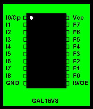
Example: GAL16V8AS (SGS-Thomson)
Pin outs
I0-I9
Inputs
Cp
Clock
OE
Output enable
F0-F7
I/O
Features:
10ns propagation delay
Fmax = 62.5Mhz
7ns max. from clock input to data output
TTL compatible 24mA outputs
Very low power: -90mA typ. (115max) Icc Half power selection, 27mA (30mA max.) eight power selection
Reconfigurable logic/reprogrammable cells
Eight output macrocells: -maximum flexibility for complex logic design -also emulates 21 types of 20pin PAL map/parametric compatibility
By Kris Heidenstrom (This email address is being protected from spambots. You need JavaScript enabled to view it.)
Release 10, 01 January 1998
This is a concise Mini-FAQ with basic information on the standard and PS/2-bidirectional PC parallel ports. As of release 9 this document exists in HTML format only. Please send any comments, corrections and suggestions to This email address is being protected from spambots. You need JavaScript enabled to view it..
In no event shall the author be liable for any damages whatsoever for any loss relating to this document. Use it at your own risk!
Introduction
A parallel port links software to the real world. To software, the parallel port is three 8-bit registers occupying three consecutive addresses in the I/O space. To hardware, the port is a female 25-pin D-sub connector, carrying twelve latched outputs from the computer, accepting five inputs into the computer, with eight ground lines (pins 18-25). Here is the pinout.
The normal function of the port is to transfer data to a parallel printer through the eight data pins, using the remaining signals as flow control and miscellaneous controls and indications. A standard port does this using the Centronics parallel interface standard.
The original port was implemented with TTL/LS logic. Modern ports are implemented in an ASIC (application-specific integrated circuit) or a combined serial/parallel port chip, but are backward compatible. Many modern ports are bidirectional and may have extended functionality. The body of this document applies only to standard ports and PS/2 ports.
The BIOS LPT Port Table
A parallel port is identified by its I/O base address, and also by its LPT port number. The BIOS power-on self-test checks specific I/O addresses for the presence of a parallel port, and builds a table of I/O addresses in the low memory BIOS data area, starting at address 0040:0008 (or 0000:0408).
The parallel port I/O address table contains up to three 16-bit words (four on some BIOSes). Each entry gives the I/O base address of a parallel port. The first word is the I/O base address of LPT1, the second is LPT2, etc. If less than three ports were found, the remaining entries in the table are zero. DOS, and the BIOS printer functions (accessed via int 17h), use this table to translate an LPT port number to a port address, to access the appropriate physical port.
The power-on self-test checks these addresses in a specific order, and addresses are put into the table as they are found, so the table will never have gaps. A particular I/O address does not necessarily always equate to the same specific LPT port number, although there are conventions.
Addressing Conventions
The video card's parallel port is normally at 3BCh. This address is the first to be checked by the BIOS, so if a port exists there, it will become LPT1. The BIOS then checks at 378h, then at 278h. I know of no standard address for a fourth port.
Direct Hardware Access
A parallel port consists of three 8-bit registers at adjacent addresses in the processor's I/O space. The registers are defined relative to the I/O base address, and are at IOBase+0, IOBase+1 and IOBase+2 (for example if IOBase is 3BCh, then the registers are at 3BCh, 3BDh and 3BEh). Always use 8-bit I/O accesses on these registers.
The bottom four bits of the control register are latched and presented on the parallel port connector, much like the data register. Three of them are inverted, so writing a 1 will output a low voltage on the port pin for them. When the parallel port is used for printing in the normal way, using the Centronics standard, these four signals are used as outputs (control signals to the printer).
These four outputs are open collector outputs with pullup resistors, so if they are set electrically high, an external device can force them low (only) without stressing the driver in the PC, and they can be used as inputs.
To use them as inputs, write 0100 binary to the bottom four bits of the control register. This sets the outputs all high, so they are pulled high by the pullup resistors in the parallel port circuitry (which are typically 4700 ohms). An external device can then pull them low, and you can read the pin states by reading the control register. Remember to allow for the inversion on three of the pins.
If you are using this technique, the control register is not strictly 'read/write', because you may not read what you write (or wrote).
Electrical signal characteristics for the three 'direction/type' types are:
Input signals are usually pulled up to +5V with a weak pullup (47K or 100K) but not on all ports!
Output signals are totem-pole or 'push-pull' outputs - i.e. they pull high and low. Some ports pull low much more strongly than they pull high. Limited current can be drawn from the outputs (typically a few milliamps per output) but the output voltage will drop as current is drawn.
OC/Pullup (open collector with pullup) outputs pull low strongly but pull high weakly. When set to electrical high, they can be pulled low externally; therefore they can be used as inputs. See control bits for more details.
Transferring Data Via the Parallel Port
The lowest common denominator parallel port is the standard (dumb unidirectional) type. Data can be transferred between such ports via a PC-to-PC parallel cable as used with INTERLNK, Laplink and FastLynx, which links five data outputs from one end to the five status inputs on the other and vice versa (see below). Data is transferred four bits at a time using the fifth bits for handshaking. This is known as nibble mode.
Another method (which will also work with all port types) links eight data bits across to five status inputs and three control lines, which are used as inputs. Other methods yielding a higher data rate can be used if both ports are bidirectional. The EPP and ECP have special hardware support for higher speeds (around 1MB/s) and the ECP also supports high-speed data transfer using DMA (direct memory addressing, a process where the hardware is able to read and write data directly to or from memory without the CPU's intervention).
File Transfer Program Cables
The parallel-to-parallel cable is used by DOS's INTERLNK program. Laplink and FastLynx cables are the same. The pin-to-pin connection between two male 25-pin D-sub connectors is: 2-15, 3-13, 4-12, 5-10, 6-11, and the reverse: 15-2, 13-3, 12-4, 10-5, and 11-6, and 25-25. This requires eleven wires. If you have spare wires, link some extra grounds together. Pins 18 to 25 inclusive are grounds. A very long cable may be unreliable; limit it to 5 metres, preferably less.
Transferring Data using Standard Parallel Ports
These sample functions use the cable described above and work with any parallel port. Data is sent four bits at a time, using the fifth lines in each direction as data strobe and acknowledge respectively. This is sometimes called 'nibble mode'.
These sample functions send and receive a byte of data. One program must be the sender, the other must be the receiver. receive_byte() will be used only on the receiver. transmit_byte() will be used only on the sender, and will not return until the byte has been received and acknowledged by the receiver. input_value() is used on both sender and receiver. In a practical program like INTERLNK, protocols are required to control the data direction and provide error checking, etc.
This program reports for LPT1, LPT2, and LPT3 whether the port exists and whether input mode can be enabled by setting the bidirectional control bit in the control register. This only works on some bidirectional ports, so the program will report non-bidirectional or in standard mode for ports that are bidirectional or enhanced, if input mode is not controlled by control register bit 5.
This program was written for Borland C. Change outportb() to outp() and inportb() to inp() for Microsoft C, I think. Save this code to BIDIR.C and compile with:bcc
The EPP (Enhanced Parallel Port) and ECP (Extended Capabilities Port) are described in the IEEE 1284 standard of 1994, which gives the physical, I/O and BIOS interfaces. Both are backward-compatible with the original parallel port, and add special modes which include bidirectional data transfer capability. These modes support fast data transfer between computers and printers, and between computers, and support multiple printers or other peripherals on the same port. In their enhanced modes, they re-define the control and status lines of the parallel port connector, using it as a slow multiplexed parallel bus. The ECP supports DMA (direct memory access) for automated high-speed data transfer.
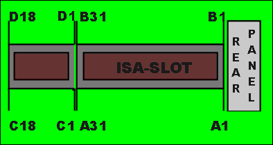
Note: "I/O pin" reffers to a pin number marked on sketch."I/O" reffers to the character of pin: I-input for system board, O-output from system board.
A1-A31
I/O pin
Signal name
I/O
A1
I/O CH CK
I
A2
SD7
I/O
A3
SD6
I/O
A4
SD5
I/O
A5
SD4
I/O
A6
SD3
I/O
A7
SD2
I/O
A8
SD1
I/O
A9
SD0
I/O
A10
I/O CH RDY
I
A11
AEN
O
A12
SA19
I/O
A13
SA18
I/O
A14
SA17
I/O
A15
SA16
I/O
A16
SA15
I/O
A17
SA14
I/O
A18
SA13
I/O
A19
SA12
I/O
A20
SA11
I/O
A21
SA10
I/O
A22
SA9
I/O
A23
SA8
I/O
A24
SA7
I/O
A25
SA6
I/O
A26
SA5
I/O
A27
SA4
I/O
A28
SA3
I/O
A29
SA2
I/O
A30
SA1
I/O
A31
SA0
I/O
B1-B31
I/O pin
Signal name
I/O
B1
GND
Ground
B2
RESET
O
B3
+5 Vdc
Power
B4
IRQ 9
I
B5
-5 Vdc
Power
B6
DRQ 2
I
B7
-12 Vdc
Power
B8
OWS
I
B9
+12 Vdc
Power
B10
GND
Ground
B11
SMEMW
O
B12
SMEMR
O
B13
IOW
I/O
B14
IOR
I/O
B15
DACK 3
O
B16
DRQ 3
I
B17
DACK 1
O
B18
DRQ 1
I
B19
REFRESH
I/O
B20
CLK
O
B21
IRQ 7
I
B22
IRQ 6
I
B23
IRQ 5
I
B24
IRQ 4
I
B25
IRQ 3
I
B26
DACK 2
O
B27
T/C
O
B28
BALE
O
B29
+5 Vdc
Power
B30
OSC
O
B31
GND
Ground
C1-C18
I/O pin
Signal name
I/O
C1
SBHE
I/O
C2
LA23
I/O
C3
LA22
I/O
C4
LA21
I/O
C5
LA20
I/O
C6
LA19
I/O
C7
LA18
I/O
C8
LA17
I/O
C9
MEMR
I/O
C10
MEMW
I/O
C11
SD8
I/O
C12
SD9
I/O
C13
SD10
I/O
C14
SD11
I/O
C15
SD12
I/O
C16
SD13
I/O
C17
SD14
I/O
C18
SD15
I/O
D1-D18
I/O pin
Signal name
I/O
D1
MEM C16
I
D2
I/O C16
I
D3
IRQ 10
I
D4
IRQ 11
I
D5
IRQ 12
I
D6
IRQ 15
I
D7
IRQ 14
I
D8
DACK 0
O
D9
DRQ 0
I
D10
DACK 5
O
D11
DRQ 5
I
D12
DACK 6
O
D13
DRQ 6
I
D14
DACK 7
O
D15
DRQ 7
I
D16
+5 Vdc
Power
D17
MASTER
I
D18
GND
Ground
I/O Channel signal description
SA0-A19 (I/O) Address bits 0 through 19 are used to address memory and I/O devices within the system. These 20 address lines, in addition to LA17 through LA23, allow access of up to 16Mb of memory. These signals are generated by microprocessor (CPU) or DMA controller.
LA17-LA23 (I/O) These signals are used to address memory and I/O devices within the system. They give the system up to 16Mb of addressability. These signals are valid when "BALE" is high.
CLK (O) This is system clock. It is synchronous microprocessor cycle with 50% duty cycle. This signal should be used only for synchronization.
RESET (O) Resetnis used to reset or initialize system logic at power-up time.This signal is active high.
SD0-SD15 (I/O) These signals provide data bus bits 0 through 15 for the microprocessor, memory, and I/O devices. SD0 is the least-significant bit and SD15 is the most-significant bit. All 8-bit devices on the I/O channel should use SD0-SD7. The 16-bit devices will use SD0-SD15.
BALE (O) (buffered) "Address latch enable" is provided by the Bus controller and is used on system board to latch valid addresses. CPU address A0-A19 are latched with falling edge of "BALE". "BALE" is forced high during DMA cycles.
I/O CH CK (I) "I/O hannel check" provides the system board with parity (error) information about memory or devices on the I/O channel. When this signal is active, it indicates an uncorrectable system error.
I/O CH RDY (I) "I/O channel ready" is pulled low (not ready) by devices to lengthen I/O or memory cycles. Any slow device using this line should drive it low immediatly upon detecting its valid address and a READ or WRITE command. Machine cycles are extended by an integral number of clock cycles.
IRQ 3-IRQ 7,IRQ 9-IRQ12,IRQ 14-IRQ 15 (I) Interrupt requests 3 through 7,9-12 and 14-15 are used to signal microprocessor that an I/O device needs attention. The IRQ-s are prioritized, with IRQ15 having the highest priority and IRQ0 having the lowest priority. An interrupt request is generated when an IRQ line is raised from low to high. The list of IRQ-s which are usually used within the system: IRQ3-COM2, IRQ4-COM1 (serial ports),IRQ 6-FDD (floppy drive), IRQ 14-hard disk.
IOR (I/O) "I/O Read" instructs an I/O device to drive its data onto the data bus. Active low.
IOW (I/O) "I/O Write" instructs an I/O device to read the data on the data bus. Active low.
SMEMR (O)-MEMR (I/O) These signals instruct the memory devices to drive data onto the data bus. SMEMR is active only when the memory decode is within the low 1Mb of memory space. MEMR is active on all memory read cycles. Both signals are active low.
SMEMW (O)-MEMW (I/O) Same as SMEMR and MEMR. besides that they are used for write data.
DRQ 0-3 and DRQ 5-7 (I) DMA Requests 0-3 and 5-7 are asynchronous channel requets uesed by peripheral devices and the I/O channel microprocessors to gain DMA services. They are prioritized, with DRQ 0 having the highest priority, and DRQ 7 having the lowest. They are active high, and they must be held high until the corresponding "DMA Request Acknowledge" (DACK) line goes active. DRQ 0-3 will perform 8-bit transfers, DRQ 5-7 will perform 16.bit transfers, DRQ 4 is used on the system board and is not available on the I/O channel.
DACK 0-3 and DACK 5-7 (O) "DMA Request Acknowledge" are used to acknowledge DMA requsets (DRQ0-7). They are active low.
AEN (O) "Address enable" signal is used to degate the microprocessor and other devices from I/O channel to allow DMA transfer to take place.When AEN is high (active) it means that DMA-controler has control of the address bus, the data-bus, Read (IOR) and Write (IOW). This means that AEN signal is available to the I/O channel as the indicator of valid CPU address. E. g. if CPU reads a data from an register within I/O device it has to provide I/O device with address of that register, with I/O Read/Write signal (I/O Read=0, I/O Write=1), and with low AEN signal (AEN=0). Only when AEN signal is low, the I/O device will be responding to CPU requests, and when AEN is high the I/O device should be detached from address and data bus (in tri-state).
REFRESH (I/O) This signal is used to indicate a refresh cycle and can be driven by a microprocessor on the I/O channel.
T/C (O) "Terminal count" provides a pulse when the terminal count for any DMA channel is reached.
SBHE (I/O) "Bus high enable" indicates a transfer of data on the upper byte of data bus, D8-D15.
MASTER (I) This signal is used with DRQ line to gain control of the system. A processor or DMA controller on the I/O channel may issue a DRQ to a DMA channel in cascade mode and receive a DACK. Upon receivinig the DACK, an I/O microprocessor may pull MASTER low, which will allow it to control the system address, data, and control lines.
MEM CS16 (I) "MEM 16 Chip Select" signals the system board if the present data transfer is a 1 wait-state, 16-bit, memory cycle.
I/O CS16 (I) "I/O 16 bit Chip Select" signals the system board if the present data transfer is a 1 wait-state, 16-bit, I/O cycle. It is active low and should be driven with an open collector or tri-state driver.
OSC (O) "Oscilator" is a high speed clock with 70 nanosecond period. This signal is not synchronous with the system clock. It has 50% duty cycle.
OWS (I) The "Zero Wait State" (OWS) signal tells the CPU that it can complete the present bus cycle without inserting any additional wait cycles.
I/O address map
Hex range
I/O Device (commonly used)
000-0FF
DMA, Interrupt controller, math coprocessor, timer and other device
170-177
AT hard disk (secondary)
1F0-1F8
AT hard disk
200-207
Game port (yostick A/D port)
278-27F
Parallel printer port 2
2C0-2DF
EGA #2
2F8-2FF
Serial port 2 ( COM 2/4 )
300-31F
Prototype card
320-32F
Hard disk (XT)
370-377
Diskette controller (secondary)
378-37F
Parallel printer port 1
3C0-3CF
Enhanced Display Adapter (EGA #1)
3F0-3F7
Diskette controller
3F8-3FF
Serial port 1 (COM 1/3)
Note: details about these devices and their control registers you can find in Tech Help V4.0 (zip file for download, size=200Kb).
Propagation delay time is defined as time needed for d. device to change states of it's outputs after changing of states has occur on it's inputs. E.G. NOT-logic device converts logic "1" at input into logic "0" at output, it would be ideal if this conversion take place immediately, but it take some time and that is our delay time. Digital device with smaller p.d. time is better, because it can operate at higher frequencies which is essential in modern digital circuits. Most common values of p.d. time in ordinary digital IC's are 10-20ns.
FAN-OUT factor
FO-factor is number which tells us how many TTL compatible devices we can connect to one output of digital device preserving voltage level of logic signals in determined range: -0.8v max for logic "0" -2.4v min for logic "1" Common value is 10 TTL-LS (it means that max. 10 d. device of TTL-LS type can be connected on one output).
Output characteristics
Outputs of digital IC's can be divided into three groups:
Bipolar outputs (TP-totem pole) are ordinary TTL outputs which can generate both logic "1" and "0".
Unipolar outputs (OC-open collector) can generate only "0" and at logic "1" the transistor is turned off and acquired voltage level is obtained by resistor connected to power. These outputs are used when is needed to connect more logic outputs on same line (bus).
Tri-state outputs (TS) have characteristics of bipolar outputs but in addition they have third state (state of high impedance) which allows them to be connected onto bus lines.
Overview of basic types of digital devices
TTL-technology (74xx) is most common technology in basic logic circuits, and it can be characterized by two basic factors: -Delay time of aprox. 20ns per logic gate. -Power consumption of cca. 15mA/logic gate
TTL-LS(low shottky: 74LSxx) is characterized by much lower power consumption then ordinary TTL preserving same operating speed: -Delay time of aprox. 20ns per logic gate. -Power consumption of cca. 4mA/logic gate
TTL-OC (there isn't special mark for those circuits but they can be identified by different number: 7400-four NAND gate, 7401-four NAND gate with open collector) these d.devices have similar properties as ordinary TTL but they have extended delay time (compared with TTL) when changing state from logic "0" to "1": cca. 50ns propagation delay time for changing from "0" to "1" and 20ns for changing from "1" to "0".
CMOS-(4xxx) technology makes possible to manufacture digital devices with very low power consumption which is main advantage of this technology: Power consumption of cca. 0.7microA/logic gate
H-CMOS (high speed CMOS: 74HCTxx) allows digital circuits to operate at higher frequencies preserving low power consumption which is main characteristic of all CMOS devices: Delay time of aprox. 8ns per logic gate.
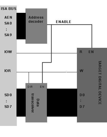
First of all your card must satisfy so called PIO data transfer protocol (Programmed I/O). This means that CPU can read or write data in/from registers on your card with simple commands such as OUT xx or IN xx (in assembler language ). Your card must correctly interpret control signals such as I/O READ/WRITE, AEN, and it must decode address from address bus to determine if CPU controller are addressing a register which reside on your card. You may decode address for your I/O registers on the card anywhere in the I/O memory area from 0FF to 3FF hex (look I/O address map) until they aren't interfere with address of other devices. E. g. if you want that your I/O register have address 3E0 you must decode that address by interpreting address lines A0 through A9 (2^10=1024=400h). Then if that address appears on the address bus you must check AEN line. If AEN is low (AEN=0), then you have to check I/O READ/WRITE signals to determine if CPU wishes to read or write data in your register. In all other cases (AEN high or not proper address on bus) your card (or it's connections) must be in so called tri-state (state of high impedance) to allow other devices on the bus to communicate with each other without interference. For better understanding here is block-scheme of ISA interface of AT-card: Block-scheme of simple ISA interface
Various analog or digital devices can be placed on your AT-card, but in order to control behavior of these devices you must have some kind of digital interface for ISA bus, as you can see on the block-scheme above, this interface can be divided in three main sections:
Target digital device is our electronic circuit which we want to place on the AT-card. Our circuit can be consists of many digital or analog devices. But this circuit must have one or more control (status) registers (which can be 1 to 16bit wide ), making possible for CPU to read out status of our circuitry or to control our circuitry.
These digital register (one or more) can be registers of A/D converter (to read out result from last conversion), or it can be Q output of JK flip-flop or something else. If your device is for example A/D converter then you don't have to use IOW line, you can use only IOR line to read out contests of A/D digital register.
Address decoder is digital circuit which decodes address of our control registers.
If we want to place our control register at address 300h (hex) then this Address decoder have to recognize this address on the address bus, generating signal called 'ENABLE' (or you can call it Chip Select CS). When this ENABLE is active, it means that CPU tries to access our control registers (CPU tries to read or write something at address 300h). ENABLE signal must enable (or select) our target digital device for reading or writing data by CPU, also it must notify Data transceiver to enable data flow from our control register to the ISA data bus.
Data transceiver is used to degate control (status) register from ISA data bus when our digital device on the AT-card is not selected (not addressed by CPU). If ENABLE signal is inactive Data transceiver must hold pins in tri-state (state of high-impedance). When CPU tries to read data from control register (ENABLE=active) on AT-card Data transceiver must direct data from control register to the ISA data bus (DIR- direction signal is low). When CPU tries to write data to control register Data transceiver must direct data from ISA data bus to the control register (DIR- direction signal is high).
As you can see the implementation of DIR signal is easy: it's connected to IOR line. Depending on type of Data transceiver, this logic for DIR signal can be altered: DIR=0->WRITE & DIR=1->READ.
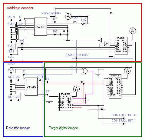
Utilizing PIO data transfer mode is very important stage in making of AT-card so to fully understand this problem I have made some trivial AT-card (on paper) as example. This AT-card example is trivial (or senseless) because it doesn't anything, but I think it quite well explains practical use of Address decoder and Data transceiver: Example AT-card
Description: This AT-card can read or write data in the register (latch 74373), precisely it can read/write only two bits from this latch (CONTROL BIT 0 and 1). These two bits can be used for control of some other device such as relay. The address of our latch register resides at 300h (hex) and we can easily set or read out these bits from our latch by simple assembler code:
MOV DX,300h ;(DX = address of our latch) MOV AL,3 ;(3dec = 0000 0011binary) OUT DX,AL ;(set: CONTROL BIT 1 = '1' and CONTROL BIT 0 = '1' ) IN AL,DX ;(reading from latch) AND AL,3 ;(reading only our two bits: AL=3 if everything is OK)
This code you can easily write in C using instructions outportb(port,value) and inportb() or you can embed this assembler code in your C program. Here is C equivalent of above assembly code: #include <dos.h> #define port_address 0x300 int value;
main() { outportb(port_address,3); value=inportb(port_address); value = value & 3; /* (filtering our two bits)*/ printf("\n Value: %u",value); /* Value:3 if everything is OK */ getch(); }
Address decoder is consists of digital comparator 74688 and partly from 7428 (four NOR gate). In practical use it's better to use 74HCT688 because of speed (ordinary 74688 has large propagation delay time). Basically this chip (74688) compares 8 digital inputs (B gate: B0-7) which are set to our desired address to another 8 digital inputs (A gate: A0-7) which are connected to the ISA address lines SA2-SA9 and when they match (A=B) output Y is active (active low). This only works when input E is active (low) or when AEN signal is low. The comparator uses only SA2-SA9 address lines which compares with value 192 (C0h or 11000000binary ). If value on SA2-SA9 matches 192 then Y output of 74688 is pulled low. The 7428 chip is consists of four NOR gate with two inputs. Inputs for first gate are marked as 1A and 1B and their output is marked as 1Y. Other NOR gates are marked in similar fashion (2A and 2B as inputs and 2Y as output for second NOR gate, etc.). Other address lines (SA0 and SA1) are decoded by NOR gate and if both are zero then output from this gate (output on 7428 chip marked as 2Y ) is high (logic '1' ). This '1' is negated and passed to the another NOR gate with Y output from 74688. If Y=0 result is '1' (output on 7428 chip marked as 1Y is '1') . This 1Y output is negated and result is ENABLE signal which is active low (ENABLE=0 -> SA0-SA9=0300h=768dec=11 0000 0000bin). As you can see our Address decoder responds with ENABLE=0 when address of our digital device (300h) appears on the ISA address bus.
Data transceiver is consist of only one chip: 74245 octal data transceiver. As you can see when ENABLE is high it's pins are in tri-state which degates our 74373 register from ISA data bus. When DIR=0 (CPU reads data from register: IOR=0) data is directed from B gate to A gate or from register to the data bus and when DIR=1 (CPU writes data to the register: IOR=1) data is directed from A gate to B gate or from data bus to the latch register.
Truth table for 74245:
E
DIR
OUTPUTS
L
L
Bus B Data to Bus A
L
H
Bus A Data to Bus B
H
X
Isolation
L = Low Voltage level H= High Voltage level X= immaterial Bus B marked on scheme: B0-B7 Bus A marked on scheme: A0-A7
Target digital device is consist of 74373 8bit register (octal transparent latch with tri-state outputs) and from one 74151 Quad 3-state noninverting buffer which is used to detach digital inputs (1D and 2D) from outputs (1Q and 2Q) of 74373 latch in write cycle. Register generates only two CONTROL bits (due to simplicity of example) which can be used for controlling other devices which can be placed on the AT-card.
Truth table for 74373:
Dn
C (LE)
OC (OE)
Qn
H
H
L
H
L
H
L
L
X
X
H
Z*
L = Low Voltage level H= High Voltage level X= immaterial Z= high impedance * note: Contest of flip-flops unaffected by state of the OC OC or OE=output enable C or LE=latch enable
Truth table for 74151:
A
G
Y
L
L
L
H
L
H
X
H
Z*
L = Low Voltage level H= High Voltage level Z*= high impedance X= immaterial G control gate (active low) A input Y output
Considering way in which our register is connected there are three operating modes of our register:
Off-line (ENABLE inactive) mode: in this mode register data outputs are enabled (OC=0) and it's possible to use our CONTROL bits 0 and 1 from register data outputs 1Q and 2Q: it's possible for other devices (which can be optionally placed on the AT-card) to use these signals.
Outputs from data transceiver 74245 are in state of high impedance (E=1) and outputs from 74151 buffer are also in state of high impedance (IOR= X immaterial and ENABLE=1 always gives 1) (signal is passed from A to Y only when control gates G of buffers are in low state (see truth table for 74151). Register inputs (1D-8D) are disabled because C=0 (only when C=high inputs can change value of our register: see truth table).
CPU reading cycle (ENABLE active & IOR=0 & IOW=1) mode: in this mode register data outputs are passed through buffer 74151 because IOR=0 OR ENABLE=0 gives 0 which enables buffer outputs and signal goes from 74373 register outputs (1Q 2Q) to inputs of data transceiver 74245 which is enabled (E=ENABLE=0 and DIR=IOR=0-->>pass signals from B gate to the A gate or D0-D7 of ISA bus), CONTROL bits are available for use by other devices in this state. Register inputs (D1-D8) are disabled because IOW=1 NOR ENABLE=0 gives 0 (only when C=high inputs can change value of our register: see truth table).
CPU writing cycle (ENABLE active & IOR=1 & IOW=0) mode: in this mode digital outputs (1Q and 2Q) from latch 74373 are detached from inputs (1D and 2D) because buffer 74151 holds outputs (1Y and 2Y) in state of high impedance (IOR=1 OR ENABLE=0 gives 1). 74373 register inputs (1D-8D) are enabled: C=1 (IOW=0 NOR ENABLE=0 gives 1) so every data which appears on inputs is stored in register as long as C control input stays high: see truth table). Data is driven from ISA data bus to the register inputs (through 74245 with DIR=IOR=1->A to the B gate), digital outputs from buffer are in state of high impedance so they not interfere with our write cycle and finally our data from CPU will appear onto register inputs (D1 D2) and it will be stored in register. Note: CONTROL bits are available for use by other devices in this state but they will change their state depending on which data is writen into register bits (1D 2D).
PIO 16 bit data transfer mode
If you want a full 16-bit data transfer you must pull down line I/O CS16 and use higher data lines D8-D15. But because there is only one I/O CS16 line on the ISA bus setting this line to 0 must take place only when our AT-card is selected for I/O operations by CPU (when ENABLE is active in previous example). IOCS16 signal driven by tri-state line driver
Use of IOCS16 isn't completely clear to me right now but I will find more info on this. There are two things that are known to me: IOCS16 line is not used in 16bit DMA transfers because 16bit DMA is selected by selection of DMA channel (channel 5-7). This fact is known to me from specifications of 8237 controller. Second thing (from ISA-bus spec.) is that 16 bit CPU transfers to 8-bit devices will be converted to two 8-bit transfers (the data on D8 through D15 will be gated to D0-D7 ).
Multiple Chip select signal
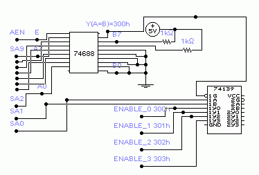
If you need to address more then one location (status or control register) on your AT card you must adapt your Address decoder to generate more then one ENABLE ( or Chip Select) signal. In our example: if we want to address four 8bit register on AT card we will use lower ISA address lines (SA0 and SA1) to accomplish that. We will put our new four registers on address:
Address
SA1
SA0
Name of signal
300h
0
0
ENABLE_0
301h
0
1
ENABLE_1
302h
1
0
ENABLE_2
303h
1
1
ENABLE_3
Address decoder with multiple ENABLE (chip select) signals
Dual demultiplexer 74139 is used for generating four ENABLE signals (ENABLE_0,1,2,3). It's convenient to use this device because we won't be needing anymore two NOR and two NOT gates. To make your card more flexible it's recommended that you always connect higher address lines (in our case SA2-SA9) through 74688 and leave lower lines (SA0,SA1) to generate multiple chip select signals. As you can see on picture it's very easy to generate four different ENABLE signals. Now it's up to us how to use these signals in conjunction with Data Transceiver and with our status registers on the AT-card.
Truth table for 74139 (labels from picture above):
IN:
1G
1A
1B
OUT:
1Y0
1Y1
1Y2
1Y3
H
X
X
H
H
H
H
L
L
L
L
H
H
H
L
H
L
H
L
H
H
L
L
H
H
H
L
H
L
H
H
H
H
H
L
L = Low Voltage level H= High Voltage level X= immaterial
Connecting IRQ-lines
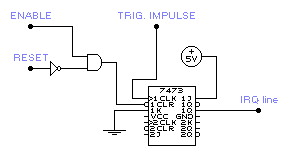
If your card uses interrupt requests, you have to connect that IRQ from your card to the IRQ on system board which is not occupied (e. g. IRQ 10).IRQ inputs are positive edge-sensitive inputs which means that IRQ is generated only when IRQ lines goes from low logical level "0" to high "1". (note: this can be altered in CMOS setup of motherboard). Why IRQ: this method is an efficient way to free up the CPU to do other important things while AT-card doesn't need attention. When AT-card needs to be served by CPU it will activate IRQ line, requesting CPU attention. CPU response to the IRQ request may be very slow (resolving priority, executing specified routines and etc.) so it is best to use IRQ interrupts as asynchronous events (generated from time to time). Therefore it's not good to use IRQ for time-critical operations demanding fast respond from CPU. If your AT-card demands fast executing of some routine by CPU in specified time (depending on state of status register on card) it's best to utilize so called Polling operate mode. Polling is simple way of checking values of status register (polling status bits) which can be done at higher speed then with IRQ routines (now our status bit acts as the interrupt signal). Characteristic of IRQ line is that our AT-card have absolute control over this line (it's not shared by other devices on ISA bus). Because of that you don't have to use digital device with tri-state ability for this line. On the other hand you must provide logic which will be able to set IRQ request and to reset IRQ line (set IRQ line to 0) when IRQ request is acknowledged by CPU. The JK bistabil (or some other flip-flop bistabil) is best for generating IRQ request: it can be triggered by some impulse and afterwards it can be easily reset to start value.
For example if your AT-card measures temperature using A/D converter (converting temperature to voltage by LM36, then voltage to the digital value by A/D) and if you want that your computer read temperature only when it reaches specified value (you don't wont that your computer continuously read out temperature from A/D register) then you can generate IRQ request. Generating IRQ request (according to this example) can be done by some comparator (digital or analog) which will generate triggering impulse which will set JK bistabil output (Q) to high level ('1').
How to generate IRQ
As you can see JK bistabil 7473 is used as flip-flop which generates IRQ request due to triggering impulse. It holds IRQ line active until our AT-card is accessed by CPU (IRQ interrupt has been acknowledged) which will set ENABLE to 0 and CLR input will clear our JK bistabil (CLR=0 > Q=IRQ=0). When computer is resetting (ISA bus RESET line=1) during power-up RESET signal will also clear JK bistabil so that IRQ will be set to 0. Note: Input data on J and K inputs is transferred to the outputs (Q and NotQ) on the negative-going edge of the clock pulse(CLK).
DMA data transfer mode
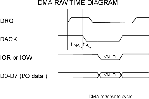
Direct Memory Access (DMA) is a type of data transfer in which the data is directly read/write into the system memory without the control of CPU, which results with greater speed of data transfer. In the DMA mode CPU is in the wait states and it is degated from data and address bus. The control of DMA-operation is obtain by DMA-controller which can handle 7-DMA channels. If your I/O device needs DMA-services (to increase speed of data transfer) you must control DACK n, DRQ n and T/C lines, where "n" represents a number of DMA channel that you want to use. You must choose free DMA channel for that purpose. (e.g. DMA channel number 2 is reserved for floppy drive). Also you have to choose between 8-bit or 16-bit DMA data transfer mode: DMA channel 0-3 are reserved for 8-bit and other channels are reserved for 16-bit data transfer mode. To initialize DMA data transfer you must program DMA-controller. E.g. you must "tell" him how many bytes is to read from your I/O registers and write to the system memory (or other way round). Important: if using DMA data transfer mode it is necessary to use IRQ logic (your device have to be able to generate IRQ interrupt) because once if DMA-transfer is initiated something can go wrong (some error occurred in our electronic circuit on the card:e.g overrun error) which will prevent AT-card to generate any more DRQ requests. In this case there is danger that DMA controller waits for DRQ request keeping DMA-channel active. Therefore our At-card can signalize error with IRQ interrupt making possible for DMA-controller to recover (to reset active DMA-channel). Number of bytes which will be transferred during DMA operation is determined by the value of T/C register (located in DMA-controller). With every DMA read/write cycle this value is decreased, and when it reaches zero the T/C signal is set active (T/C=1). DMA-controller registers are on the address 000-01F and 0C0-0DF, and you can access them directly or by DOS/BIOS routines (assembler language). When you initiate DMA data transfer your I/O device have to generate a DRQ n requests when it is ready to send or receive data from/in system memory. Also it have to continuously check out the condition of DACK n and T/C lines. After issuing a DRQ signal I/O device must wait for DACK signal to goes active. Only when DACK signal is active the I/O device can drive its data to data bus (or read data from data bus in DMA read cycle). After this DMA-controller takes care where to put that data in system memory (that address in system memory is defined before in initiation process ). During DMA operations AEN line is active (1) and it is used to disable selection of an I/O device when DMA address is on the address bus. The I/O device (AT-card) selection should be determined by the DMA acknowledge outputs for the that channel. (E. g. if AT-card uses DMA channel number 3, when DACK3 line is set by DMA controller AT-card should be 'aware' of that signal). When the T/C line is set active it means that DMA-data transfer operation has ended. Note: T/C signal is set active during last DACK "n" to notified the I/O device that T/C signal is Terminal Count signal for DMA channel number "n" (explanation: on ISA-bus there is a only one T/C line, and there are 7 DMA channels which can be active at same time). To make example how to implement DMA-data transfer on AT-card is too complicated for explanation ( I'm afraid that nobody will understand that) therefore I will show only time diagrams for DMA operation:
This picture shows one-byte (D0-7) DMA transfer in which data is transferred while DACK signal is active (DACK=0).During that time At-card must enable it's data outputs (valid data is on the ISA data bus) and it must properly recognize IOR and IOW signals. As you can see our card generates DRQ signals (high level), DMA controller responds with DACK signal active (DACK=0).Delay time marked as 'tMA' (time in which DACK=0 after DRQ=1) have maximum value which is determined by us. We determine max. time in which DMA-controller must respond to our DRQ request and if DMA-cont. fails to respond in that time (so called overrun error) our AT-card should terminate DMA-operation issuing IRQ interrupt (resetting active DMA-channel). For better explanation: Floppy drive controller (FDC 7265) in DMA read transfer mode reads data stored on the diskette. Due to rotating of diskette every consecutive byte on diskette have to be read in cca. 13 microseconds. Therefore maximum value of 'tMA' should not exceed 13 microseconds. If DMA-cont. exceeds this time, new byte will be read by FDC and previous byte will be lost. Our data is now corrupted and FDC terminates DMA-operation issuing IRQ. After DACK=0 AT-card have to reset DRQ (DRQ=0) line in time defined by 'tA' (maximum value of tA) and this value is 140ns for FDC 7265.
Conclusion
These are the basic of how to make your AT-card. When you assembling your AT-card you must take care about various things such as time-delays of your logic circuits, power dissipation, OC (open collector) and tri-state abilities of logic circuits. About time-delays: ISA bus operates at 8Mhz even on newest motherboard because of compatibility to older I/O devices (speed of PCI divided by factor 4 ). Therefore every PIO or DMA cycle (read or write) can not be faster then 8Mhz regardless on CPU speed. Every digital circuit from ordinary 74xxx family can operate up to 20Mhz but this depends on type of circuit. If digital circuit is more complex such as our digital comparator 74688 then it is better to use faster chips from HCT family (almost every digital chip from 74xxx serie has HCT equivalent). This section is made to help out everybody who needs help in getting started in designing AT-cards for PC-compatible. Later I will add some program examples on how to make IRQ handlers, how to program interrupt controller, how to program DMA cont. and etc..
Author: Before 15 years ago, Internet was hard to search/reach and there were no quality info (Google wasn't invented) so I spent lot of time digging out the specifications of various electronic circuits. All data collected is summarized on these pages. Nowdays, all this information is almost obsolete, and I kinda lost interest in electronics, but nevertheless I will leave these pages as they were.
Tomi Engdahl page: very useful page at which you can find docs on various things such as: electronic circuits (audio,video,computer,data communication circuits,..), description of opamps (LMxxx), 555 timer chip,MAX232 chip for RSs232 communication, there is also description of PC-hardware: ISA,PCI bus, Plug'n Play technology...

 IOCS16 signal driven by tri-state line driver